
 | Наукова періодика України | 
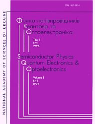
| Semiconductor physics, quantum electronics & optoelectronics |
Sukach A. V. Carrier transport mechanisms in reverse biased InSb p-n junctions / A. V. Sukach, V. V. Tetyorkin, A. I. Tkachuk // Semiconductor physics quantum electronics & optoelectronics. - 2015. - Vol. 18, № 3. - С. 267-271. - Режим доступу: http://nbuv.gov.ua/UJRN/MSMW_2015_18_3_7 The linearly-graded p-n junctions were prepared by diffusion of cadmium into n-InSb(100) substrate with the electron concentration <$En~symbol Ы~1,6~cdot~10 sup 15 ~roman cm sup -3> at the temperature T = 77 K. Passivation and protection of mesa structures have been carried out using thin films of CdTe. Forward and reverse current-voltage characteristics were investigated within the temperature range 77...156 K. It has been found that the total dark current consists of generation-recombination and tunneling current components, which are dominant at high (T = 120...156 K) and low (T << 120 K) temperatures, respectively. Experimental results have been explained using the model of a nonhomogeneous p-n junction. It has been shown that in the linearly-graded p-n junction with the rather thick (~<$E1~mu m>) depletion region tunneling current flows through the states related to dislocations in the depletion region. The performed estimation of electrical parameters of diffusion InSb p-n junctions allows to predict behavior of InSb-based photodiodes at operation temperatures T >> 77 K.Carrier transport mechanisms have been investigated in linearly graded InSb p-n junctions prepared using thennal diffusion of Cd into single crystal substrates of n-type conductivity. The investigations were focused on the reverse current as a function of bias voltage and temperature. The obtained experimental data show that local inhomogeneities in the depletion region are responsible for the excess tunneling current observed in the reverse biased junctions. The inhomogeneities have been attributed to dislocations, precipitates or other extended defects. A phenomenological model is proposed to explain experimental data. Цитованість авторів публікації: Бібліографічний опис для цитування: Sukach A. V. Carrier transport mechanisms in reverse biased InSb p-n junctions / A. V. Sukach, V. V. Tetyorkin, A. I. Tkachuk // Semiconductor physics quantum electronics & optoelectronics. - 2015. - Vol. 18, № 3. - С. 267-271. - Режим доступу: http://nbuv.gov.ua/UJRN/MSMW_2015_18_3_7.Додаткова інформація про автора(ів) публікації: (cписок формується автоматично, до списку можуть бути включені персоналії з подібними іменами або однофамільці) |
|
|
Всі права захищені © Національна бібліотека України імені В. І. Вернадського |
|||||